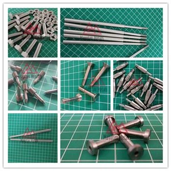
What are ion implanted parts used for?
An ion-implanted piece refers to a semiconductor material that has undergone a critical and precise process known as ion implantation. This process involves the introduction of dopant atoms into the semiconductor material using high-energy ion beams, resulting in the deliberate alteration of its electrical properties. Ion-implanted pieces serve as the foundational material for the fabrication of integrated circuits (ICs) and other semiconductor devices, playing a pivotal role in defining the electrical characteristics and performance of the resulting electronic components.
The process of ion implantation begins with the preparation of the semiconductor material, which is typically in the form of a wafer made of silicon. This initial preparation includes cleaning the surface of the wafer to remove impurities and contaminants, ensuring uniform implantation and efficient doping. Additionally, the semiconductor material may undergo specific treatments to optimize its crystalline structure and surface characteristics, preparing it for the ion implantation process.
Once the preparation stage is complete, the semiconductor material is loaded into a highly specialized piece of equipment known as an ion implanter. The ion implanter is designed to administer precise and controlled doses of dopant atoms using high-energy ion beams. This equipment allows for the selective introduction of dopant atoms into the semiconductor material, enabling the customization of its electrical properties according to the specific requirements of the intended electronic devices.
The ion implantation process involves several crucial parameters that determine the characteristics of the ion-implanted piece. These parameters include the choice of dopant species, the energy of the ion beam, the dose of implanted ions, and the spatial distribution of the doping profile within the semiconductor material. By carefully adjusting these parameters, semiconductor manufacturers can tailor the conductivity, carrier concentration, and junction characteristics of the ion-implanted piece, thereby influencing the behavior and performance of the electronic components fabricated from it.
One of the primary functions of ion implantation is to introduce dopant atoms into the semiconductor material to modify its electrical conductivity. By selectively implanting dopant atoms into specific regions of the wafer, semiconductor manufacturers can create regions with different doping levels and types, effectively controlling the conductivity and carrier concentration within the material. This capability is fundamental for the development of transistors, diodes, and other essential components of electronic devices, as the electrical characteristics of these components depend on the precise control of doping profiles within the semiconductor material.
In addition to modifying conductivity and creating junctions, ion implantation plays a crucial role in tailoring the dopant profiles of the semiconductor material. The precise control over the distribution of dopant atoms within the ion-implanted piece enables semiconductor manufacturers to achieve specific electrical characteristics, such as threshold voltages, breakdown voltages, and carrier mobilities, essential for the proper functioning of electronic devices. This level of customization allows for the production of semiconductor materials with highly tailored electrical properties, meeting the stringent requirements of modern electronic applications.
Furthermore, ion-implanted pieces are essential for the development of specialized semiconductor devices, including power electronics and optoelectronic components. The ability to tailor the electrical properties of semiconductor materials through ion implantation is crucial for creating high-performance power devices, such as insulated-gate bipolar transistors (IGBTs) and high-voltage diodes. Additionally, ion implantation is employed in the manufacturing of optoelectronic devices like photodetectors and light-emitting diodes (LEDs), where precise control over the dopant profiles and junction characteristics within the ion-implanted piece is essential for achieving the desired optical and electrical properties.
In conclusion, ion-implanted pieces represent semiconductor materials that have undergone the critical process of ion implantation, enabling the precise customization of their electrical properties for the production of integrated circuits, semiconductor devices, and specialized electronic components. Through the selective introduction of dopant atoms using high-energy ion beams, ion implantation allows semiconductor manufacturers to tailor the conductivity, junction characteristics, and dopant profiles of the ion-implanted piece with precision and control. This level of customization is essential for meeting the demanding performance requirements of modern electronic devices and facilitating the development of advanced semiconductor technologies.