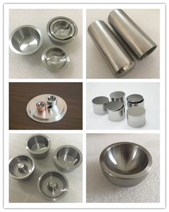
What is the specific application of tungsten in semiconductor barrier layers and why?
What are the properties of tungsten?
1,High Melting Point: Tungsten has an exceptionally high melting point of around 3,400 degrees Celsius, which is crucial for semiconductor fabrication processes that involve high-temperature steps. The high melting point ensures the stability and integrity of the tungsten barrier layer during various manufacturing processes.
2,Diffusion Resistance: Tungsten demonstrates excellent diffusion resistance, particularly in the context of copper diffusion barriers. Copper is commonly used as an interconnect material in integrated circuits, but it tends to diffuse into neighboring layers, leading to device failure. Tungsten serves as an effective barrier layer to prevent the interdiffusion of copper and other materials, preserving the device's structure and functionality.
3,Chemical Stability: Tungsten exhibits strong chemical stability, making it resistant to reactions with other materials used in semiconductor processes. This property allows tungsten barrier layers to maintain their integrity and performance over time.
4,Electrical Conductivity: While primarily used as a barrier layer, tungsten still boasts good electrical conductivity. This characteristic ensures that the barrier layer does not impede the efficient flow of electrical signals within the semiconductor device.
5,Hermetic Seal: Tungsten is also utilized as a barrier layer to create a hermetic seal, particularly in applications where protection against oxygen and moisture is critical. By depositing a thin layer of tungsten, semiconductor devices are shielded from the detrimental effects of oxygen and moisture, such as degradation and accelerated aging.
What are the specific applications of tungsten in semiconductor barrier layers?
Tungsten is frequently utilized as a barrier layer in semiconductor technology due to its inherent characteristics. Here are some specific applications of tungsten in semiconductor barrier layers:
1,Copper Diffusion Barrier:
Tungsten acts as a reliable barrier layer between copper (Cu) and other materials in semiconductor devices. Copper is an excellent conductor but tends to diffuse into neighboring materials, leading to performance and reliability issues. Tungsten's diffusion resistance prevents the migration of copper atoms, ensuring the integrity and functionality of the device.
2,Oxygen and Moisture Barrier:
Tungsten is employed as a barrier layer to protect sensitive semiconductor components from the harmful effects of oxygen and moisture. By depositing a thin layer of tungsten, semiconductor devices are shielded from the ingress of these contaminants, enhancing their overall reliability and lifespan.
3,Etch Stop Layer:
Tungsten is also used as an etch stop layer during semiconductor fabrication processes. It is deposited between different layers of the device and acts as a boundary that halts the etching process at a specific point. This precise control over the etching process enables the creation of complex device structures with high accuracy.
4,Adhesion Layer:
Tungsten serves as an adhesion layer between different materials, promoting strong bonding and minimizing delamination issues. It enhances the adhesion of subsequent layers to the underlying substrate, ensuring the structural integrity of the device.