

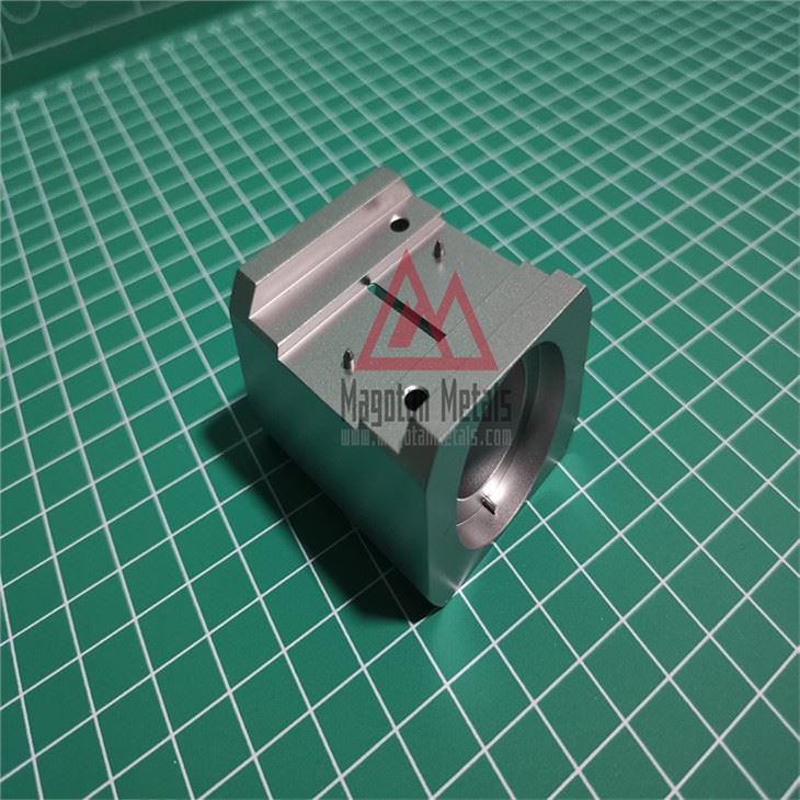

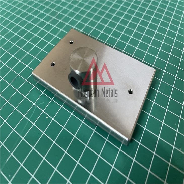
Ion Implantation Spare Parts
Applications of ion implantation components:
(1) ion implanter
(2) semiconductor equipments
Product Introduction
1. Product name: Ion Implantation Spare Parts
Ion implantation technology is a pure surface treatment technology, it does not need to be carried out in a high temperature environment, so it will not change the shape and surface finish of the workpiece. Magotan can provide tungsten ion implantation spare parts and molybdenum ion implantation spare parts.


2. Specifications of Ion Implantation Spare Parts:
Item name | Ion Implantation Spare Parts |
material | W, Mo, TZM, MLa, Ta, Ceramic, Graphite |
Model | OEM No. |
| For ion implanter | Applied Materials, Axcelis,Varian, AIBT,Nissen, Sen, Ulvac |
3. The method of ion implantation is to accelerate impurity ions in a vacuum and low temperature (for Si, voltage ≥105 V), and the impurity ions with large kinetic energy can directly enter the semiconductor; at the same time, some lattices will also be generated in the semiconductor. Therefore, low-temperature annealing or laser annealing is required to eliminate these defects after ion implantation. The impurity concentration distribution of ion implantation generally exhibits a Gaussian distribution, and the highest concentration is not at the surface, but at a certain depth within the surface.
3.1 The advantage of ion implantation is that it can precisely control the total dose, depth distribution, and surface uniformity of impurities, it is a low-temperature process (to prevent the re-diffusion of the original impurities, etc.), and it can realize self-alignment technology (to reduce capacitance effects).
3.2 In the process flow, the next step in lithography is etching or ion implantation. During ion implantation, where there is photoresist protection, the ion beam cannot penetrate the photoresist; where there is no photoresist, the ion beam can be implanted into the substrate to achieve doping. Therefore, the photoresist used in the ion implantation process must be able to effectively block the ion beam.
3.3 In the front-end manufacturing process of integrated circuits, there are many photolithography layers followed by ion implantation. These photolithography layers are called ion implantation layers. After the ion implantation is completed, the photoresist on the surface of the wafer must be removed. Removing the photoresist after ion implantation is a difficult point in the photolithography process. Requirements for the removal process include:
(1) Cleanly and thoroughly remove the photoresist on the substrate;
(2) Try to avoid damage to the surface of the substrate, especially the ion implantation area (that is, the area without a photoresist);
(3) Try to avoid damage to the device (such as the metal of the gate).
4. The ion implanter is also a key device in the pre-fabrication process of integrated circuits. In order to change the carrier concentration and conductivity type, the semiconductor needs to dope the area near the semiconductor surface. Compared with the conventional thermal doping process, ion implantation can improve the implantation dose, The implantation angle, implantation depth, lateral diffusion, and other aspects are precisely controlled so that ion implantation is widely used in semiconductor manufacturing.
Ion Implanter Classification | |||
Category | Energy Range | Implant Dose Range | Main Applications In The Process |
Low Energy Large Beam Ion Implanter | The ion beam current is greater than 10mA, the extreme value is 25mA, and the beam energy is less than 120keV. | 1013-1016cm-2 | Source-drain implantation, polysilicon gate implantation, etc. |
High Energy Ion Implanter | The beam energy exceeds 200keV, and the extreme value is around 5MeV. | 1011-1013cm-2 | deep-buried layer |
Medium And Low Beam Ion Implanter | The ion beam current is greater than 10mA, and the beam energy is less than 180keV. | 1011-1017cm-2 | Lightly doped drain region, SmartCut penetrates the barrier layer, etc. |
5. Our Company and Factory
Magotan has a complete raw material production line and self-produced tungsten, molybdenum, materials as the quality basis, and can design, produce and process high-precision high-quality ion implantation spare parts according to customer requirements; can provide large beam, medium beam tungsten and molybdenum products for current and high-energy ion sources; can provide tungsten high-energy ion source parts, tungsten or molybdenum large-beam ion implantation parts, and molybdenum medium-beam ion source parts. And our products specification is complete, the performance is reliable, with the high quality at low price. We have won the general customer trust.
Hot Tags: ion implantation spare parts, China, suppliers, manufacturers, factory, buy, price, discount, in stock, made in China
You Might Also Like


Send Inquiry
