


Tungsten Components For Ion Implantation
Semiconductor Ion Implantation Parts:
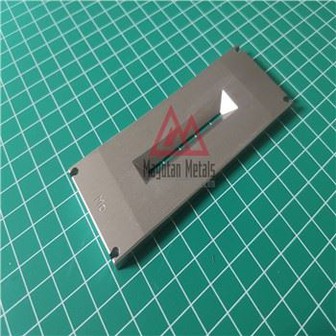
tungsten ion implantation components
Molybdenum OEM consumable parts
tantalum ion implantation parts
Boron Nitride ion implantation parts
Ceramic ion implantation parts
Product Introduction
Tungsten components for ion implantation application
In the electronics industry, tungsten components for ion implantation has become an important doping technology in the microelectronics process, and also an important means to control the threshold voltage of MOSFET. Therefore, it can be said that it is an essential means to manufacture large-scale integrated circuits in modern times.
The method of ion implantation is to accelerate the impurity ions (for Si, the voltage is ≥105 V) in vacuum and low temperature, and the impurity ions with large kinetic energy can directly enter the semiconductor; At the same time, some lattice defects are generated in the semiconductor, so after ion implantation, annealing at low temperature or laser annealing is required to eliminate these defects. The impurity concentration distribution of ion implantation generally presents a Gaussian distribution, and the highest concentration is not at the surface, but at a certain depth within the surface.
The advantage of ion implantation is that it can precisely control the total dose, depth distribution and surface uniformity of impurities, and it is a low-temperature process (can prevent the rediffusion of original impurities, etc.), and can realize self-alignment technology (to reduce capacitance effect).
The next step in the process is etching or ion implantation. In ion implantation, where there is a photoresist, the ion beam cannot penetrate the photoresist. Where there is no photoresist the ion beam can be injected into the substrate to achieve doping. Therefore, the photoresist used in the ion implantation process must be able to effectively block the ion beam.
Many photolithography layers in IC front process are performed while the ion implantation is performed. These photolithography layers are called implant layers. After ion implantation, the photoresist on the wafer surface must be removed, which is a difficult problem in the lithography process. Requirements for the cleaning process include:
(1) Clean and thorough removal of photoresist on the substrate;
(2) Try to avoid the damaged surface of the substrate, especially the ion-injected area (i.e. the area without photoresist);
(3) Try to avoid damage to the device (such as the metal of the gate).
Tungsten components for ion implantation show


Tungsten components for ion implantation Video Show
Magotan metals are semiconductor ion implantation parts manufacturer who has committed to production of tungsten components for ion implantation, Molybdenum OEM consumable parts and tantalum ion implantation parts for years. We use high quality raw material which gurantee the high purity of 99.95%, with excellent product performance. Accept sample first.
FAQ

Hot Tags: tungsten components for ion implantation, China, suppliers, manufacturers, factory, buy, price, discount, in stock, made in China
You Might Also Like


Send Inquiry